December 16, 2019

Alebrijes - Lectura p.127-129


Lectura corta, páginas 127-129. Excelente libro para disfrutar en compañía de tu ser querido, cuenta la historia del artesano cartonero Pedro Linares López inventor de los Alebrijes en México del siglo XX.

Consíguelo aquí: https://amzn.to/34YcKNN

December 12, 2019

AFM Training - Tip functions

Responsible research: Dr. Francisco Flores 
Day: 2 

Today I observe how a point for AFM is changed: We need to choose it depending on the material and the measurement we want to perform. For example, the sample of today is gold nanoparticles over a glass substrate then we have tried the TAP300Al-G which is a probe from the company BudgetSensors. This probe is designed for AFM in Tapping mode and is coated with reflective aluminum. 

From the company BudgetSensor, we can discover the function of the tip models: 

  • No coating: is designed for topography purpose 
  • Backside aluminum coating: is designed to enhance the laser reflectivity and ensure stable measurement form highly reflective surfaces. 
  • Backside Gold coating (inertness):  is designed for stable reflection measurement in liquids. 
  • Overall coated Gold: is designed and used for Biological Samples and aggressive chemical ambients. Often use for TIP functionalization.  
  • Cr and Pt coated probe: is designed for electrical measurement like electrostatic force microscopy. 
  • Diamond-like carbon coating: enhance the durability of the tip and is designed to perform many consecutive scans 

Here are some photographies from the training day: 

Figure 1: Change of Tip for AFM Measurement in Bruker Dimension Edge 

Figure 2: Responsible researcher placing the tip in the AFM equipment 


Figure 3:  Getting the sample inside (gold nanoparticles deposited on glass substrate) 

December 10, 2019

What are preprints?


Preprint vs traditional paper submission.  When I was pursuing my bachelor's degree I went to a research center and the first thing I read there was "Science that is not shared is not science" then I had the opportunity to enter this fascinating world of thinkers, conquers or discoverers. 

But, How to share science? There are two ways one is peer review paper manuscript where you are reporting to science community your research this way time schedule is important In my experience  1 year of research is resume in a manuscript which is submitted to the Journal and there peers review can last from 1 - 8 months for a response. If this is favorable the publishing date is scheduled but if not correction suggestion should be made before.  

How about pre-print? This way is new for the community, Actually, my doctoral and postdoctoral advisor are not using it. That's why I am here. Looking on the internet for ideas. We can take advantage of this new method. For sure, sharing new discoveries is the idea of science communication, but the opportunity to have feedback is amazing.  Because in that way is how knowledge is built. 

Feel free to watch the video. Now we need to discover where is the adequate server for preprint submission (at the same time as the peer review journal submission).

Cornel University: Arxiv.org 

  • Condensed Matter (Solid state physics) - Link 
    • physics.optics
    • cond-mat.mtrl-sci
    • physics.app-ph
  • ChemRxiv: The Preprint Server for Chemistry

December 09, 2019

AFM training: Bruker Dimension Edge at IFUAP

Responsible research: Dr. Francisco Flores 
Day: 1

First training day on AFM Bruker Dimension Edge AFM at the Physics Institute of BUAP. This equipment will allow the measurement of topography properties like roughness and grain size. The researcher in charge explains too that it's possible to acquire electrical conductivity and work function from the surface of the films. 


Model: AFM - Bruker Dimension Edge 

Close up of AFM equipment


Connection block card: National Instrument BNC 2110 

December 06, 2019

Alebrijes - Libro de Cecilia Reyes


Lectura corta, páginas 47-49. Excelente libro para disfrutar en compañía de tu ser querido, cuenta la historia del artesano cartonero Pedro Linares López inventor de los Alebrijes en México del siglo XX. Consíguelo aquí: https://amzn.to/34YcKNN
-- Un homenaje a la creación del artesano mexicano Pedro Linares López quien en un trance cercano a la muerte tuvo la visión de animales tenebrosos que no eran de este mundo y que más tarde, gracias a su imaginación y a la magia de sus manos, fue capaz de traer a la realidad. "Alebrijes alebrijes", escuchó que gritaban en su sueño.

December 05, 2019

Laboratory - Bismuth Sulfide thin films

Location: Physics Institute of BUAP, Puebla, Pue.  
Chemical deposition:  Bi2S3 Bismuth Sulfide
Supervisor: M.C Denisse Loeza 

Chemical deposition of bismuth sulfide from the master thesis work of M.C. Denisse Loeza. This work has the intention to develop new materials (semiconductors) for solar cells. Like the ternary compound Cu3BiS3, which posses potential properties as a p-type semiconductor for absorber layer on thin-film technology. 

Fig.1: Washing Bi2S3 thin films after chemical deposition


Fig.2: Dry using N2 gas 

Fig.3:  Another angle showing the base where the glass substrates are held. 

November 17, 2019

Advance Materials group at IFUAP-BUAP

Dra. Mou Pal group: Research and development of metal chalcogenides, metal oxides nanoparticles. ( Happy Birthday ) From left to right: Andres, Marifer, Cancino, Dra. Mou Pal, Denise, Me (Jesus Capistran).  

Is it hard to get a postdoctoral stay in Mexico?


Coffee cup at IFUAP-BUAP (From MIT) 
In Mexico, 2019 is a hard year for Science and technology due to two main reasons: a) Change of Mexican president followed with a change of political flagship and b) Corruption priority besides economical aspects.

This year I had the opportunity to apply for a postdoctoral fellowship from Conacyt-International to spend one year at EMPA-Switzerland.  In August, the results came and I was not selected. These results are followed by a reduction of federal found for Conacyt and the government bet for carbon-based fuels. 

Fortunately, I had a plan B. I apply for a postdoctoral fellowship at the BUAP founded by the program SEP-PRODEP.  The process for a stay from PRODEP is really slow, the application opens in February and closes the last day of September.  The problem is the results they come from a minimum time of 3 months. In my case, the results came after 6 months of wait.

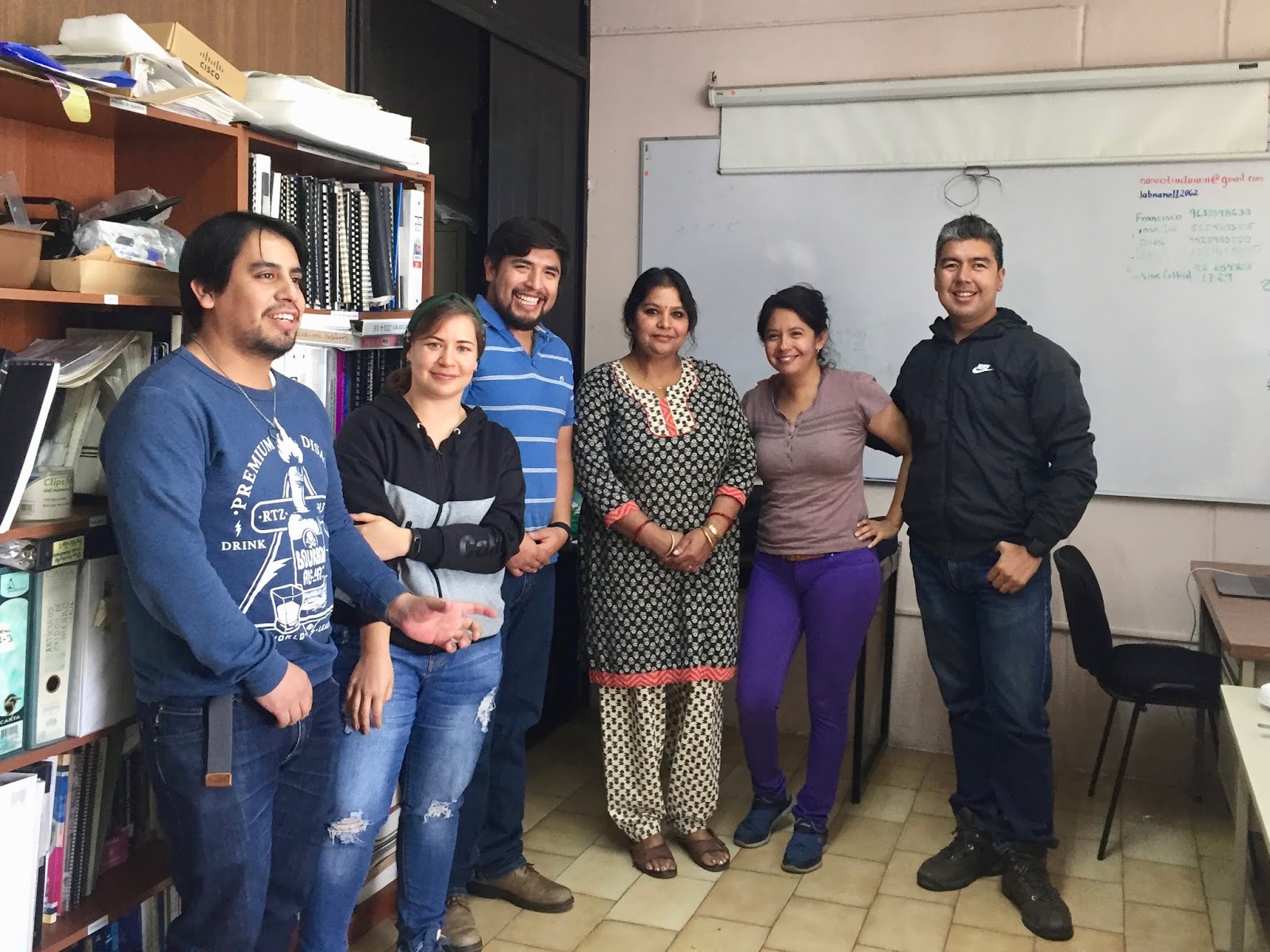
Last week IFUAP-BUAP give the results they accept my stay but I should move quickly to Puebla City.  For that reason here I am taking a cup of coffee from the cafeteria at IFUAP.  How a great surprise they give me before the winter season. I feel great in one of the best institutions and universities in Mexico for superior education or bachelor grade.

If you are a  new 2019-postdoctoral working in Mexico please tell us: How was your experience getting that position? If you are interested in a postdoctoral position, please check these three opportunities:
Note: 
You are allowed to apply for the three in a row during the year. Do it and don't lose opportunities. 

November 01, 2019

How to get Project Management skills for Scientists

Photo by Nathan McBride on Unsplash
I have the opportunity to be the Solar Semiconductors Morelos (StartUp) founder partner, this young company gives me the profile of an entrepreneur looking for opportunities related to the energy sector. Last days I had the chance to reach the industry, government, and academic actors. Here,  I realize there will be a push (investment) for new projects related to the acquisition of renewables on companies and government. But, How a scientist can touch this sector?
A scientist is a person who creates and solve problems using science and technology
A scientist solves problems using scientific methodology and international scientific literature. However,  the question is How a scientist fits on a company with no research department? When I ask for advice from a businessman, he said that I should know what kind of job I am looking for.  For example, doing a job search at Tesla Company, I found jobs for Energy Analysts. This job is located in the Operation and Business section, and the requirements can be fit for people with a bachelor's degree.

Going to the industry from a science profile means to pivot to engineering  or going to an entrepreneur adventure on innovation. 

If we analyze the path of a scientist who wants to become an entrepreneur doing innovation, then some skills are needed, like business and management. Here is why the need for project management certification.  In this era, there is a lot of information, but it needs to be trusting information; that's why I will use and recommend EDX for online preparation. (About EDX Micromasters®)

1. EDX Platform offers a free online course (information), but the certification has a low cost. It is essential to acquire knowledge and skills, but if you have the financial support, a certification shows the company your skills.  Here is a MicroMaster, ® on Project Management skills, need if you a scientist wants to become an entrepreneur.

RITx Project Management MicroMasters® Program


  • Project management: Life cycle 
  • Best practices for project management success
  • International project management
2. PMI.ORG - Online courses.  This entity is the international  Project Management Institute that offers preparation courses and certification for project managers. I am not getting a course here, but I will look for the PMBOOK® Guide and Standards (English), you cand find here the Spanish version: Gúia del PMBOOK®"


The purpose here after reading this book is to acquire the project management language. Are you looking for the same skills?  Let me tell you about my experience at the next meeting with the businessmen.  But for now, What are you looking for? Are you an entrepreneur scientist? 

October 30, 2019

Job Interview - Cluster Puebla - Artifex Angels

Yesterday, I had the fortune to meet three founders of Artifex Angels at Titanium Tower. When I get to the lobby, the next message can be read on the wall.
Titanium tower provides business space solutions to medium and large firms. It offers a strategic location for international business in Mexico as well as a unique setting for entrepreneurs.
What a great message for an entrepreneur researcher (academic) because I found a place where real businesses are done, and maybe after this job interview, I could begin the path to become a business leader on innovation in the renewable energy sector.  

This place makes me realize I have new dreams to catch as an entrepreneur seeking and promoting the acquisition of renewables, or as one of the founders said, you could be an articulator (linker) between industry and the hubs for new business. 

What do you think was the result of the job interview? 

https://drive.google.com/uc?export=view&id=1bqpObYCFLrEkk-k6ZltKSu_ojLtgEpXs


October 21, 2019

Hub de innovación tecnológica: Eficiencia energética y Energías Renovables

Step by step, we should lead the science from the university labs to the marketplace. There will be no opportunities if you don't seek them.  Solar Semiconductors Morelos will attend this meeting looking for strategic partners inside the industry and technical collaboration with GIZ and the  Queretaro innovators.


References:

October 17, 2019

Hobby: Lectura El Libro Salvaje (extracto)


Extracto del libro salvaje , primer capítulo ( Separación) del autor Juan Villoro
Lector: Jesús Capistrán Libro en Amazon:
https://amzn.to/2pwJPAw

October 15, 2019

How to read a scientific paper in just three steps

Reading on paper is an old school way to annotate
and highlight the most interesting elements
For a scientist, reading is a must responsibility in the modern world of information, this task allows us to update the state of the art of the current research. For example, the objective of my work is to reproduce and improve antimony sulfo-selenide thin-film solar cells. Therefore, the first thing I did before experimental research It was to read the updated literature. As I am in touch with the author of the paper of interest I asked him about it's last published paper where their group develops Sb-S-Se photovoltaic mini-module prototypes. 

P.K. Nair*, J.D.G. Sánchez, L.G. Martínez, P.Y.G. Ayala, A.K.M. Peñaloza, A.B. León, Y.C. García, J. Campos Álvarez, M.T.S. Nair, Chemically Deposited Antimony Sulfide Selenide Thin Film Photovoltaic Prototype Modules, ECS J. Solid State Sci. Technol. 8 (2019) Q89–Q95. doi:10.1149/2.0101906jss.

To fully understand, I almost read a scientific paper three times:

  • First: Print it or read it on PDF (Mendeley could help), the important thing here is to read from the beginning to the end as soon as possible.
  • Second: Make annotations for later discussion and highlights from the most important elements you can find on the text.
  • Third: Write a resume, this will allow you to save the essential information in the same notebook of literature review. I prefer to write it on the Blogspot or a note on the Evernote app following the next template.

Read more, to discover the structure or template for paper review, here you are going to write just the notes and highlighted parts. This is my way to learn fast. If you have an alternate strategy please feel free to share it in the comments section.

October 14, 2019

Paper: Chemically deposited antimony sulfide selenide thin film photovoltaic prototype modules


Authors: P. K. Nair,  José Diego Gonzaga Sánchez, Laura Guerrero Martínez, Perla Yoloxóchitl García Ayala, Ana Karen Martínez Peñaloza, Alessandra Beauregard León, Yareli Colín García, José Campos Álvarez, and M. T. S. Nair

Link: ECS Journal of Solid State Science and Technology, 8 (6) Q89-Q95 (2019)


Abstract

We present thin film antimony sulfide selenide prototype photovoltaic modules of area, seven cm2 and conversion efficiency (η) of 3.5%. The thin films of Sb2SxSe3-x (x, 0.8–1.6) of 120–180 nm in thickness were deposited on FTO/CdS(80 nm) substrates at 80°C from chemical bath containing potassium antimony tartrate, thioacetamide and sodium selenosulfate. Thin film of CdS of 80 nm in thickness was deposited from a chemical bath at 80°C during 65 min on fluorine-doped SnO2 (FTO). The solar cell structure FTO/CdS/Sb2SxSe3-x/C had colloidal graphite paint of area, 0.7 cm× 0.7 cm. This cell structure was heated at 300°C during 30 min in a nitrogen ambient to create a carbon-doped antimony chalcogenide layer. Silver paint was applied to the carbon electrode and on FTO around it. Prototype modules had seven series connected cells of one cm2 each with a total area of seven cm2. Solar cell with varying composition of Sb2SxSe3-x along its thickness had a η of 3.88% at an open circuit voltage (Voc) of 0.44 V and short circuit current density of 18.3 mA/cm2. Prototype modules lighted-up blue light emitting diodes at a power, 5–15 mW.


Highlights

  • The best solar cell is:   Voc = 441 mV, Jsc = 18.34 mA/cm2, FF = 0.48 and efficiency = 3.88 % measured under standar conditions of 1 sun (Solar simulator). 
  • Application of carbon paint over chalcogenide layer and subsequent heating of the entire cell structure would create a carbon-doped antimony chalcogenide layer


Device fabrication 
  • Substrate:  TEC7 
  • Window layer:  CdS by chemical deposition (80 nm)
  • Absorber layer: Sb-S-Se by sequential chemical deposition  (180 nm)
  • Back contact: Graphite paint (SPI) / Silver paint (N2 heat treatment, 300 ºC) 

Characterization techniques 

  • EDS - Over finished solar cells 
  • GIXRD - Over solar cell 
  • T and R - Optical  for calculation of absorption coefficient, bandgap  and photogenerated current (JL) 
  • JC curve for solar cell and mini-modules
  • EQE for solar cells 

Notes: 

  • This work is open for improvements in all the constitutive components of the solar cell device. 


October 03, 2019

Fabrication of Titanium dioxide as a compact layer for Perovskite and thin-film solar cells

Special thanks for Dra Hailin Zao Hu at IER-UNAM who let me collaborate and learn from their group the methodology for TiO2 compact layer deposition.  All the training was possible with the assistance of Ph.D. student Fabian and undergraduate  Ing. Gabriela Abrego from UTEZ.

Preparing TCO with magic tape  for HRT layer deposition 

Spin coater  and micropipette are the essential tools for TiO2 deposition 

First heating of the compact layer over a hot plate : low temperature

Second and final heating - Sintering TiO2 on a muffle furnace : high temperature

Compact TiO2 layer deposited over a TCO for thin-film chalcogenide or Perovskite solar cells. 


August 27, 2019

Talking about strategies for high efficiency kesterite solar cells

Dr. Edgardo A. Saucedo visits BUAP after the MRS congress in Cancun, Mexico and gives us a motivational talk about kesterites PV technology. He is the leader of the Solar Energy Materials and Systems Group at IREC and leads the European STARCELL project too.

 Kesterites are a promising PV material, it's metal elements, Copper, Zinc, and Tin are abundant on earth crust. This material owns a tetragonal lattice similar to commercial PV technology. As Dr. Saucedo said, they come from the royal family of photovoltaics. 
Kesterites comes from the royal family of photovoltaics


Source: PV-Education Crystal structure of the royal family of photovoltaics

The pace of research on kesterites has been slow due to the emergence of perovskites who has reached a conversion efficiency of 24%(early 2019) while kesterite holds a record of 12.6% reported by IBM in 2013. As you can see, there is a difference of 6 years between both reports [1].

STARCELL born to push forward kesterites PV technology and it is formed by universities and industrial partners. As you can see in the next image, the project is conceived by institutions which have the infrastructure for developing solar cells. You can read a complete description in the following link (About Starcell-Project)
STARCELL organization structure for CZTS development of solar cells and scale-up to PV modules
Challenges of kesterite technology: Doping and alloying 

The main technological challenge of kesterites is their Low Voc.  For example, the sulfo-selenide kesterite or CZTSSe has a Voc of 513 mV [2] compared to commercial CIGSe solar cells which reach 734 mV [3].  Dr. Saucedo said that some bulk properties of the kesterite related to recombination process should be enhanced controlling the following techniques:


August 26, 2019

IFUAP - Physics Institute BUAP (POSDOC)

Last April 2019, I wrote a project for a postdoctoral stay at IFUAP. This stay will be founded by PRODEP-SEP. The goal is to reinforce the photovoltaic area developing thin-film solar cells based on novel materials. The application specifies a 3-month deadline for a response (late July). However,  when the deadline arrives, IFUAP said that this response can spend up to  5-months with no compromise. Therefore, this project can not be started.  

All of this is happening due to political reason. When the Mexican government changes most of the funds for public scientific research were frozen until politics trace the new route of investment. Somebodies say that it is due to a re-structure of the funds, but nobody can deny the collateral damage. There are a lot of unemployed people who were founded by Conacyt during their master or a Ph.D. degree.

No matter this situation, I embraced the risk and moved to Puebla City. Here I have been able to meet the researcher, its infrastructure, and the surroundings. BUAP is the Autonomous University of Puebla one of the best of this city.  After three weeks, I have been able to assist the weekly seminars (open to the public), interact with bachelors and Ph.D. Students.  When I saw for the first time the main IFUAP building, I could understand that the university is in a current expansion. They are building its Rectoria Tower.  I'll expect a positive response from IFUAP to be able to do science within collaboration with their specialist. 

Meanwhile, let's discover the history of Puebla located in their museums. And of course, prepare a short manual for solar cells design using SCAPS-1D software.


Fig 1: IFUAP  - Institute of physics - BUAP (Puebla) 


Fig 2: Profile measurements of thin films (co-work and training) 

August 15, 2019

Chemical deposition of antimony sulfide & silver antimony sulfide

The following photographs show the first 30 minutes of the solution reaction for chemical deposition of antimony sulfide thin films. This material is a p-type semiconductor. It is deposited as an amorphous source (Sb-S). The films have the necessary content to produce an orthorhombic lattice after heating above 250 ºC.

Application

Antimony sulfide is used for the research of thin-film solar cells with the following configuration TCO/CdS/Absorber/BackContact.  This film is achieved using the formula reported in the paper I publish during my Ph.D. program (With no AgNO3).  Find it here.

For tips about deposition, feel free to write a comment!


[1] J. Capistrán Martínez, P.K. Nair, Photoconductive thin films of AgSbS2 with cubic crystalline structure in solar cells, Physica Status Solidi (a). 212 (2015) 2869–2876. doi:10.1002/pssa.201532496.

Initial deposition condition temperature near 10 ºC

The reaction of the Sb-S solution begins after 10 minutes. 

The color of the reaction change completely at 30 minutes, this color will be maintained until the controlled precipitation finish. 

After 3-4 hours of deposition, the films look good, there is adherence to the glass substrate and specular reflection in the surface. 

July 11, 2019

Water molecule using Burai 1.3 and Quantum Espresso

Course: Electronic properties of semiconductors by AB-INITIO  

Profesor: Dr. Raciel Jaimes López  (Postdoctoral at IER-UNAM) 


Simulation of water molecule formation using Burai 1.3 and Quantum Espresso
Viewer by Jmol
Last month I attended the course Electronic properties of semiconductor by AB-Initio at IER-UNAM, on the 1st day we had a quick view about the background of DFT (Density Functional Theory), plane waves and pseudopotentials. During the course, we learn about the open-code Quantum Espresso software which is used for electronic-structure calculation and materials modeling at nano-scale.
Here I share the  methodology I follow for the example water-molecule    

  1. Install  BURAI1.3 on MAC (includes Quantum-Espresso)
  2. Install MPI for MAC
  1. Open BURAI  and choose examples/XYZ: Water molecule (H2O.xyz)


June 07, 2019

12% de eficiencia en el primer curso taller de Perovskitas Híbridas (IER-UNAM)


TCO/c-TiO2/m-TiO2/Perovskite/HTM/Au 

Ultimo día de curso-taller de fabricación de celdas solares de perovskitas hibridas. Al final del día el grupo del primer curso con la asesoría del grupo de investigación de perovskitas de IER-UNAM logró obtener una eficiencia de conversión de 12% en área activa de 0.1 cm^2.  El grupo de investigación  a cargo de la Dra. Hailin Zao de IER-UNAM al día de hoy ha logrado eficiencia record del 18%. 


Galeria "Fabricación de celdas solares de perovskita hibrida"


Curso intensivo del 3 al 7 de Junio de 2019 en IER-UNAM sobre Fabricación de celdas solares de perovskita hibrida. (Educación continua).

Estructura: TCO/c-TiO2/m-TiO2/Perovskite/HTM/Au